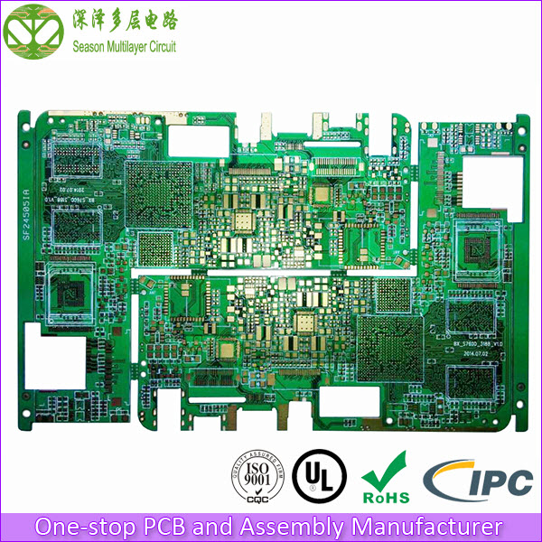
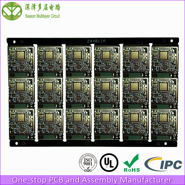
What's the purpose of heavy copper Circuit Board? One of them is to meet high power device requirement. The thicker copper on PCB, the work power is higher, but how heavy requires? It depends on your unique product need. The small heavy copper pcb generally is hard to make since it is easy to twist and wrap after profile making. We can do it since we know how to panelize the board and use what method to make the profile.
Specialized in one-stop PCB and Assembly
manufacturing, Heros Electronics is committed to providing quick-turn high
quality HDI PCB and PCBA to our customers all over the world with affordable price.
Every circuit board is fabricated as per strictest standards in compliance to IPC
class II, IPC class III, UL, RoHS and others, which ensures the PCB board and
product assembly is done to exceed the requirement of customers.
Why Choose
Us?
-
Professional PCB fabrication team
-all engineers have years’ experience in PCB manufacturing field
-
Advanced equipment and high
precision inspection & testing tools
-
Top raw materials including CCL
(Copper Clad Lamination), chemistry, and solder mask ink & legend ink
-
Skilled operators with good command
of all CCPs (Critical Control Points)
-
Full set of surface finish
equipment can do ENIG, immersion silver, immersion Tin, OSP, HASL (lead
free), plating gold and plating silver without outsourcing risk.
-
Cutting edge printed circuit
board manufacturing process capacities
-
Max aspect ratio reaches to 10
: 1
-
Max copper weight on double PCB
surface can reach to 6OZ
-
The thickness of solder mask
can control to 50μm
-
Min Impedance control value is
50ohm +/- 5%
-
Min NC drilling diameter 0.2mm
and min laser drilling diameter is 0.1mm
-
Circuit board manufacturing
strictly as per IPC standards and make sure 100% qualified
-
Strictly perform PDCA (Plan-Do-Check
Action Cycle) process, and continuously improve product performance
-
Leading outstanding enterprise
of energy saving and environmental protection
And demand of heavy copper pcb, click here for quick quote.