Home / Products / PCB Fabrication / HDI PCB
HDI PCB
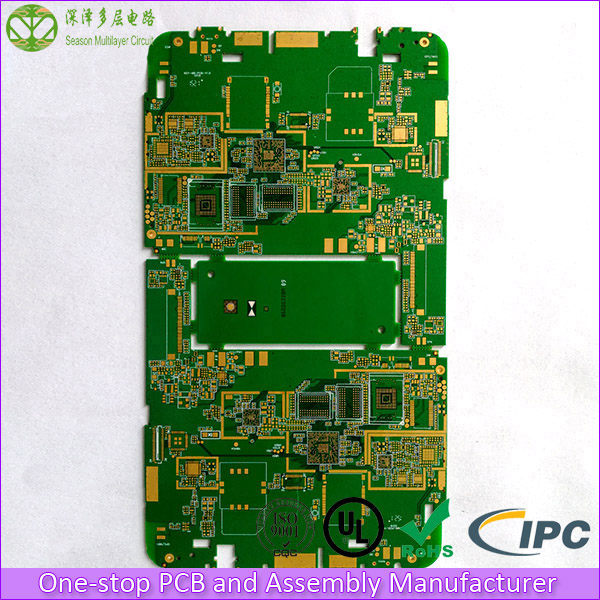
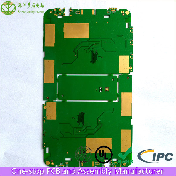
Quick Turn PCB for Pad with Shengyi S1141 and 1+N+1 Blind Microvias
Layer Count: 8L
Board Thickness: 1.0mm
Panel Dimension:190*86mm/2up
Material: S1141
Copper on board surface: 35μm
Min Hole Diameter: 0.1mm
Min line Width/Space: 8/8mil
Surface Finish: ENIG+Selective OSP in BGA area<
Product Details

1 (44)


1 (42)


This quick turn PCB is manufactured for electronic Pad application. The requirement includes 1 stage 0.1 buried and blind microvias, immersion gold together with selective OSP finish in the BGA areas, and 50ohm +/- 5% impedance control. 


Microvias PCB are becoming more and more common in high density board designs of today. We provide quick turnkey PCB service. There are many benefits to laser drilling microvias, including real estate savings, impedance control, circuit reliability, and RF line termination. For this reason, we have developed microvia laser drilling processes to work with a very wide range of materials and via profiles to fit your designs that meet IPC standards. Heros Electronics offers laser microvia drilling in both copper clad and unclad laminates. While we do recommend that outer layer foils be kept to half ounce or thinner for process efficiency, we are capable of handling much thicker copper cladding if your design calls for them.


Specialized in one-stop PCB and Assembly manufacturing, Heros Electronics is committed to providing quick-turn high quality HDI PCB and PCBA to our customers all over the world with affordable price. Every circuit board is fabricated as per strictest standards in compliance to IPC class II, IPC class III, UL, RoHS and others, which ensures the PCB board and product assembly is done to exceed the requirement of customers.


Why Choose Us?

  1. Professional PCB fabrication team -all engineers have years’ experience in PCB manufacturing field
  2. Advanced equipments and high precision inspection & testing tools
  3. Top raw materials including CCL (Copper Clad Lamination), chemistry, and solder mask ink & legend ink
  4. Skilled operators with good command of all CCPs (Critical Control Points)
  5. Full set of surface finish equipment can do ENIG, immersion silver, immersion Tin, OSP, HASL (lead free), plating gold and plating silver without outsourcing risk.
  6. Cutting edge printed circuit board manufacturing process capacities
  7. Max aspect ratio reaches to 10 : 1
  8. Max copper weight on double PCB surface can reach to 6OZ
  9. The thickness of solder mask can control to 50μm
  10. Min Impedance control value is 50ohm +/- 5%
  11. Min NC drilling diameter 0.2mm and min laser drilling diameter is 0.1mm
  12. Circuit board manufacturing strictly as per IPC standards and make sure 100% qualified
  13. Strictly perform PDCA (Plan-Do-Check Action Cycle) process, and continuously improve product performance
  14. Leading outstanding enterprise of energy saving and environmental protection

And demand of HDI PCB, click here for quick quote.

返回顶部

在线客服系统