What Is Rapid PCB Prototyping
The electronics industry thrives on innovation, where the ability to transform ideas into functional products swiftly often determines market success. At the heart of this accelerated development lies rapid PCB prototyping—a game-changing service that bridges the gap between concept and reality. This article explores the fundamentals, processes, applications, and transformative impact of rapid PCB prototyping in modern electronics.
Ⅰ.Defining Rapid PCB Prototyping
Rapid PCB prototyping refers to the expedited manufacturing of printed circuit board samples to validate designs, test functionality, and identify flaws before mass production. Unlike traditional PCB fabrication, which can take weeks, rapid prototyping delivers functional boards in 24–168 hours, enabling engineers to iterate designs quickly and cost-effectively.
Key Characteristics
- Speed: Turnaround times reduced by 70–90% compared to conventional methods.
- Flexibility: Supports small batches (as few as 5–10 units) and complex designs.
- Precision: Advanced manufacturing techniques ensure micron-level accuracy.
- Cost Efficiency: Early error detection slashes post-production fixes by up to 80%.

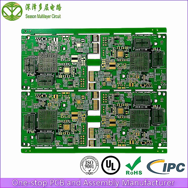
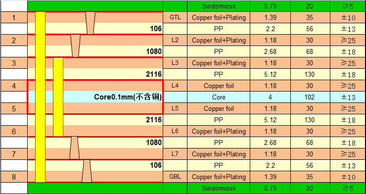
Core PCB
Layer Count: 8L
Material: FR4 Tg150
Material: 1.6mm
Panel Size: 129.2*82.6mm/2
Outer Layer Copper Thickness: 1OZ
Inner Layer Copper Thickness: 1OZ
Min Via Diameter: 0.20mm
Trace Width/Spacing: 3/4mil
Min BGA Pad: 0.25mm
Surface Finish: 1-2U’’ENIG
8 layer core pcb,A compact, high-performance core component for smart devices. Features user-friendly design, simplified maintenance, and enhanced operational efficiency.
Ⅱ.The Rapid Prototyping Workflow: 7 Critical Steps
1. Design Optimization
Using tools like Altium Designer or KiCad, engineers create digital schematics while adhering to Design for Manufacturing (DFM) principles:
- Component Placement: Minimizes trace lengths to reduce signal delay.
- Thermal Management: Positions heat-sensitive parts away from power components.
- Signal Integrity: Avoids crosstalk by isolating high-frequency traces.
Example: A robotics team redesigned a motor driver layout in 2 hours to eliminate EMI issues.
2. Material Selection
Substrate and conductive materials are chosen based on application needs:
- FR-4: Standard epoxy laminate for consumer electronics.
- Aluminum Core: Dissipates heat 8x faster than FR-4 (ideal for LED lighting).
- Flexible PCBs: Polyimide films for wearables like smartwatches.
- High-Frequency Laminates: Rogers RO4350B for 5G antennas.
3. File Preparation
Designers export industry-standard files:
- Gerber Files: Define copper layers, drill holes, and silkscreen markings.
- Bill of Materials (BOM): Lists components for assembly.
- Drill Files: Specify hole sizes and coordinates.
4. Advanced Fabrication
Manufacturers employ cutting-edge technologies:
- Laser Drilling: Creates microvias as small as 50μm (thinner than a human hair).
- Direct Imaging: UV lasers transfer circuit patterns with ±10μm accuracy.
- ENIG Finish: Electroless nickel immersion gold ensures reliable soldering.
5. Quality Assurance
Prototypes undergo rigorous checks:
- Automated Optical Inspection (AOI): Scans for missing traces or misaligned pads.
- X-Ray Imaging: Verifies layer alignment in multilayer boards.
- Impedance Testing: Ensures signal integrity in high-speed designs.
6. Functional Testing
Engineers simulate real-world conditions:
- Power Cycling: Tests durability under 1,000+ on/off sequences.
- Environmental Stress: Exposes boards to extreme temperatures (-40°C to +125°C).
- Signal Analysis: Measures rise/fall times with oscilloscopes.
7. Iterative Refinement
Feedback loops drive continuous improvement:
- A drone manufacturer revised prototypes 5 times to reduce weight by 20%.
- A medical startup optimized sensor placement to enhance signal accuracy.

Computer PCB
Layer Count: 8L
Material: FR4 Tg170
Board Thickness: 1.6mm
Panel Size: 159*136mm/4
Outer Layer Copper Thickness: 1OZ
Inner Layer Copper Thickness: 1OZ
Min Via Diameter: 0.20mm
Min BGA Pad: 0.25mm
Trace Width/Spacing: 3.8/3.2mil
Surface Finish: ENIG2U’’
8 layer computer pcb,An 8 layer computer peripheral PCB based on the RK3399 solution, designed for intelligent auxiliary systems.
Ⅲ.Applications Transforming Industries
1. Accelerated Product Development
- Case Study: A smart thermostat startup used 3 iterations in 10 days to fix a Wi-Fi connectivity issue, cutting time-to-market by 6 months.
2. Production Line Validation
- Factories test assembly workflows using prototypes to:
- Calibrate pick-and-place machines.
- Optimize solder paste application.
3. Technical Education
- Universities use prototypes for:
- SMD soldering workshops.
- IoT project kits (e.g., Raspberry Pi add-ons).
4. Low-Volume Manufacturing
- Customized solutions for niche markets:
- Industrial IoT sensors (100-unit batches).
- Vintage audio equipment repairs.
5. Startup Innovation
- Entrepreneurs leverage rapid prototyping to:
- Build crowdfunding prototypes (e.g., Kickstarter campaigns).
- Test market viability with beta units.
Ⅳ.Why Rapid Prototyping Matters
| Factor | Impact |
|---|---|
| Speed-to-Market | Launch products 60% faster than competitors |
| Cost Savings | Fixing a design error pre-production costs 1,000**‌ vs. ‌**10,000+ post-production |
| Risk Mitigation | Identifies 95% of flaws before mass production |
| Sustainability | Reduces material waste by 75% vs. traditional methods |
Ⅴ.The Future of Rapid Prototyping
Emerging technologies are pushing boundaries:
- 3D-Printed Electronics: Combine circuitry and structural components in a single print.
- AI-Driven Design: Algorithms auto-optimize layouts for signal integrity and thermal performance.
- Same-Day Global Shipping: Partnerships with logistics firms enable 24-hour worldwide delivery.
By 2025, experts predict that 80% of PCB prototypes will be ordered, manufactured, and shipped within 24 hours, further democratizing access to advanced electronics development.

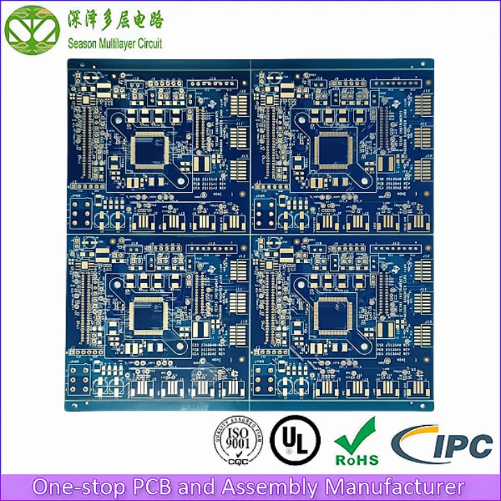
PCB prototyping
Layer Count: 4L
Material: FR4 Tg150
Board Thickness: 1.6mm
Panel Size: 162.56*159.86mm/4
Outer Layer Copper Thickness: 1OZ
Inner Layer Copper Thickness: 1OZ
Min Via Diameter: 0.20mm
Trace Width/Spacing: 4/4mil
Surface Finish: 2U’’ENIG
Automotive-grade PCB compliant with halogen-free requirements. Designed for automotive electronic components, offering stable performance, cost-effectiveness, fast lead time , and premium technical support.
Conclusion
Rapid PCB prototyping is not merely a manufacturing service—it’s the backbone of modern electronics innovation. By enabling engineers to test ideas fearlessly, iterate relentlessly, and deliver products faster, it empowers industries ranging from healthcare to aerospace. In an era where technological advancements occur at breakneck speed, rapid prototyping ensures that groundbreaking ideas don’t languish on paper but instead evolve into tangible, market-ready solutions. Whether you’re a student building your first circuit or a Fortune 500 company developing next-gen AI hardware, rapid PCB prototyping is the catalyst that turns vision into reality.


