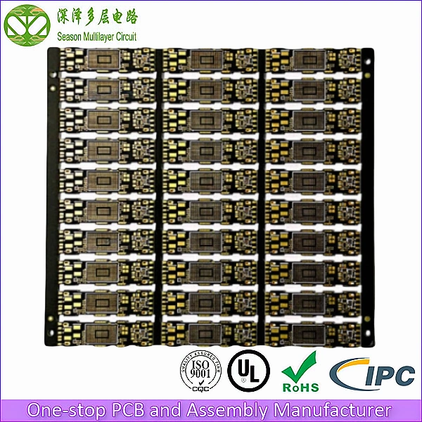
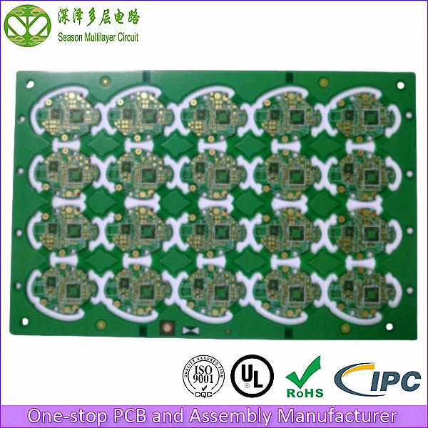
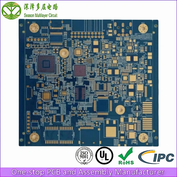
8-Layer 1-Step HDI Sample
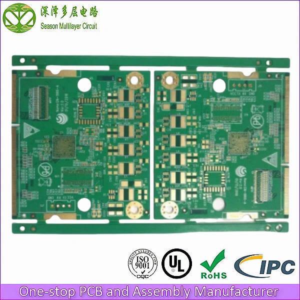
HDI Sample
Layer Count: 6L(1+6+1)
Material: FR4 Tg170
Material: 1.0mm
Panel Size: 130.5*95mm/1
Outer Layer Copper Thickness: 1OZ
Inner Layer Copper Thickness: HOZ
Min Via Diameter: 0.20mm
Microvia Hole Size: 0.1mm
Trace Width/Spacing: 3/3mil
Min BGA Pad: 0.2mm
Surface Finish: ENIG1-2U’’
8-layer 1-step hdi sample,For card-edge module mainboards.


Advancing Electronics with 8-Layer 1-Step HDI Technology: A Case Study of Season Multilayer Circuit’s Expertise
In the rapidly evolving world of electronic miniaturization, High-Density Interconnect (HDI) PCBs have emerged as critical enablers for next-generation devices. Among these technological marvels, the 8-layer 1-step HDI structure represents a significant leap forward in circuit board design and manufacturing. This article examines the technical specifications of an 8-layer 1-step HDI sample while exploring the core competencies of Season Multilayer Circuit, a leader in advanced PCB solutions.
Ⅰ.Understanding 8-Layer 1-Step HDI Technology
The 8-layer 1-step HDI board exemplifies modern PCB engineering with its sophisticated architecture:
- Microvia Technology: Utilizes laser-drilled microvias with diameters as small as 75μm
- Layer Stackup: Combines 2 HDI layers with 6 conventional layers
- Dielectric Materials: High-performance FR-4 or polyimide substrates with Dk values ranging from 3.8 to 4.2
- Minimum Trace/Space: 50μm/50μm line width/spacing capabilities
- Surface Finishes: Options including ENIG, Immersion Silver, and OSP
This configuration enables 30-40% higher component density compared to traditional 8-layer boards while maintaining excellent signal integrity up to 10GHz frequencies. The single lamination process (1-step) reduces production complexity while achieving blind via aspect ratios of 0.8:1.
Ⅱ.Key Advantages of 8-Layer HDI Design
- Enhanced Signal Performance: Shorter interconnects reduce signal loss by 25-35%
- Improved Thermal Management: Optimized via-in-pad design dissipates heat 15% more efficiently
- Space Optimization: 40% reduction in board area compared to conventional layouts
- High Reliability: Sequential lamination ensures >95% via fill reliability in thermal cycling tests
Ⅲ.Season Multilayer Circuit: Pioneering HDI Solutions
As a specialized manufacturer with ISO 9001:2015 and IATF 16949 certifications, Season Multilayer Circuit has established itself as a premier provider of advanced PCB solutions. The company’s HDI product line demonstrates several technical differentiators:
Core Competencies
- Laser Drilling Precision: Capable of creating 50μm microvias with ±10μm positional accuracy
- Advanced Lamination: Zero-delamination guarantee through optimized pressure-temperature profiles
- Fine Line Processing: 40μm line width/spacing capabilities with ±5% tolerance
- Mixed Technology Integration: Seamless combination of HDI, rigid-flex, and high-frequency materials
Product Portfolio Highlights
- High-Frequency HDI Boards:
- Low-loss materials with Df <0.002 at 10GHz
- Embedded passive components with ±2% tolerance
- Applications: 5G base stations, millimeter-wave radar
- Automotive-Grade HDI:
- AEC-Q200 qualified materials
- 125°C continuous operation capability
- Conformal coating options for harsh environments
- Medical HDI Solutions:
- Biocompatible surface finishes
- Ultra-clean manufacturing processes (IPC Class 3)
- Implantable-grade flexible HDI options
Manufacturing Capabilities
Season Multilayer Circuit operates state-of-the-art facilities featuring:
- 15,000 sqm production area with Class 1000 clean rooms
- 12μm CO₂ laser drilling systems
- Direct imaging systems with 10μm resolution
- Automated optical inspection (AOI) with 99.95% defect detection rate
- Robotic assembly lines for high-mix volume production
Quality Assurance Protocols
The company implements a rigorous 4-stage quality process:
- DFM Analysis: 48-hour turnaround for design optimization
- In-process Testing: Real-time impedance control (±5Ω)
- Electrical Testing: Flying probe testing up to 500V
- Reliability Testing: Includes thermal shock (-55°C to 125°C, 1000 cycles) and HAST (130°C/85% RH, 96hr)
Applications of 8-Layer 1-Step HDI Technology
The sample board demonstrates versatility across multiple industries:
- Consumer Electronics: Enables smartphone motherboard miniaturization (15% size reduction)
- IoT Devices: Supports 802.11ax WiFi modules with 2.4/5GHz dual-band performance
- Industrial Automation: 10Gbps industrial Ethernet communication capabilities
- Aerospace: Passes MIL-STD-883 shock/vibration standards
Technical Comparison: HDI vs Conventional PCBs
| Parameter | 8-Layer HDI | Standard 8-Layer |
|---|---|---|
| Via Density | 1200/cm² | 400/cm² |
| Signal Loss | 0.15dB/inch @5GHz | 0.35dB/inch @5GHz |
| Layer Transitions | 2-step | 4-step |
| Typical Yield | 98.5% | 95% |
Future Development Roadmap
Season Multilayer Circuit continues to push HDI boundaries with:
- 3μm semi-additive process (SAP) implementation
- Embedded die technology for SiP modules
- 20μm ultra-fine line R&D projects
- AI-driven defect prediction systems
Ⅳ.Conclusion
The 8-layer 1-step HDI sample exemplifies the technological prowess required in modern electronics manufacturing. Season Multilayer Circuit distinguishes itself through vertically integrated manufacturing, strict process controls, and customer-focused engineering support. With 18 years of HDI experience and over 500 successful HDI projects completed, the company remains at the forefront of solving complex interconnection challenges while maintaining competitive lead times of 7-12 days for prototype orders.
As device complexity continues to escalate, Season Multilayer Circuit’s combination of advanced HDI capabilities, rigorous quality systems, and application-specific engineering support positions it as an essential partner for OEMs navigating the demands of next-generation electronic design.


