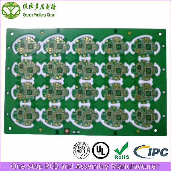
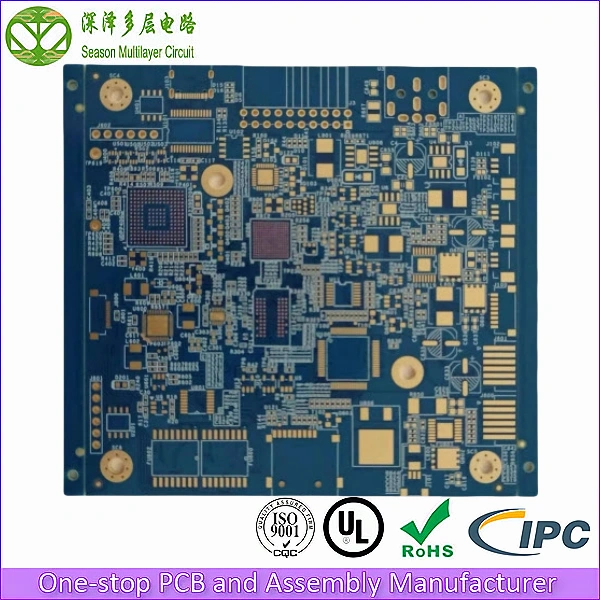
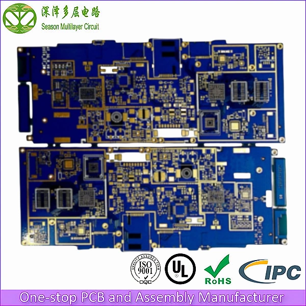
6-Layer 2-Step HDI Sound Card PCB
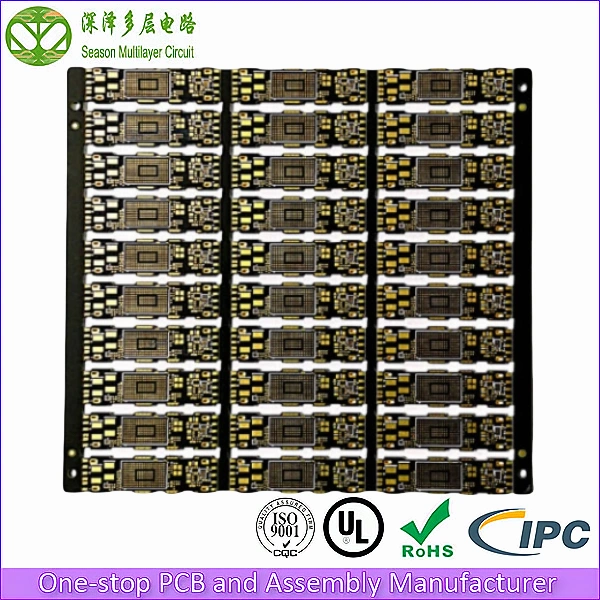
HDI Sonud Card PCB
Layer Count: 6L(2+2+2)
Material: FR4 Tg170
Material: 1.6mm
Panel Size: 116.5*106.4mm/30
Outer Layer Copper Thickness: 1OZ
Inner Layer Copper Thickness: HOZ
Min Via Diameter: 0.20mm
Microvia Hole Size: 0.1mm
Trace Width/Spacing: 3/3mil
Min BGA Pad: 0.2mm
Surface Finish: ENIG1-2U’’
A 6-layer 2-step HDI sound card PCB, designed for audio processing in computers, audio systems, mobile phones, and related applications.

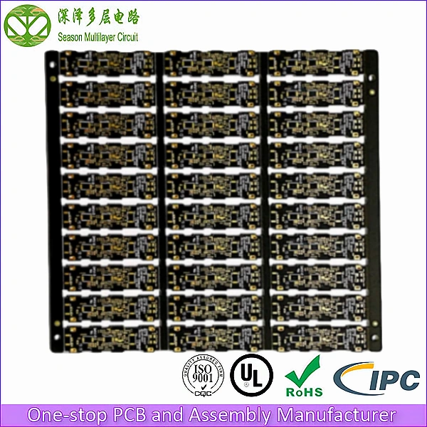
Sound Card PCB: Optimized Design and Innovative Technologies for Superior Audio Performance
In the era of digital audio, the HDI sound card PCB (Printed Circuit Board) serves as a critical component in computers for processing audio signals. Its design and technological innovations directly impact audio signal transmission quality, conversion accuracy, and overall user experience. This article explores the significance of sound card PCBs, key design considerations, and their transformative effects on audio performance.
I. The Critical Role of Sound Card PCBs
The HDI sound card PCB lies at the heart of audio technology, responsible for processing, converting, and transmitting audio signals.
- Digital-to-Analog Conversion (DAC): Converts digital audio signals from the computer into analog signals for playback through speakers or headphones. High-precision DAC circuitry ensures signal accuracy and fidelity.
- Signal Conditioning: Amplifies, filters, and reduces noise in audio signals to enhance clarity and dynamic range.
- System Integration: Provides interfaces for seamless communication with other computer components, enabling bidirectional audio input/output.
II. Key Design Considerations for HDI Sound Card PCBs
Successful HDI sound card PCB design hinges on four pillars: circuit layout, material selection, manufacturing processes, and interface scalability.
1. Circuit Layout Optimization
- EMI/RFI Mitigation: Strategic trace routing minimizes electromagnetic interference (EMI) and radio-frequency interference (RFI), preserving signal integrity.
- Thermal Management: Optimized component placement reduces heat generation, ensuring long-term reliability.
2. Material and Process Innovations
- Low-Loss Substrates: High-purity copper traces and low-dielectric-loss base materials (e.g., FR-4, polyimide) minimize signal attenuation.
- Advanced Manufacturing: Multilayer PCB stacking and laser-drilled microvias enhance signal density and impedance control.
3. Scalable Interface Design
- Versatile Connectivity: Supports multiple I/O interfaces (3.5mm jacks, USB-C, optical S/PDIF) for compatibility with headphones, microphones, and professional audio equipment.
III. Impact of HDI Sound Card PCBs on Audio Experience
1. Audio Fidelity Enhancement
- High-Resolution Audio: 24-bit/192kHz DACs and ultra-low-jitter clocks reproduce nuanced musical details.
- Noise Suppression: Active shielding and ground plane isolation reduce harmonic distortion (THD < 0.001%).
2. Feature-Rich Functionality
- Immersive Soundscapes: Supports Dolby Atmos, DTS, and virtual surround sound for gaming and cinematic experiences.
- Smart Audio Control: Integrated DSPs enable voice assistant compatibility and real-time EQ adjustments.
3. Future-Proof Expandability
- Modular Design: PCIe/Thunderbolt interfaces allow upgrades for studio-grade AD/DA conversion and multi-channel mixing.
IV. Breakthrough: 6-Layer 2-Step HDI Technology
The adoption of 6-layer 2-step HDI (6L2S HDI) technology marks a paradigm shift in sound card PCB design:
- Enhanced Signal Integrity: Additional layers reduce crosstalk and impedance mismatches, critical for high-frequency audio signals.
- Thermal Efficiency: Symmetrical stackup (e.g., 0.8 mm core + 1080 PP prepreg) improves heat dissipation, enabling stable operation under heavy loads.
- Manufacturing Precision: Sequential lamination and 1/3 oz copper foil (12μm) ensure consistency in ultra-fine trace fabrication (3/3 mil line/space).
Typical 6-Layer 2-Step Stackup:(1+1+2+1+1)
| Layer | Material | Thickness |
|---|---|---|
| Soldermask | ≥5um | |
| L1 | 1/3oz +Plating | 35±10μm |
| Blind hole through the layer | 1080 PP Prepreg | 72 μm |
| L2 | 1/3oz +Plating | ≥15 μm |
| Blind hole through the layer | 1080 PP Prepreg | 72 μm |
| L3 | 1/3oz +Plating | ≥15 μm |
| Buried Microvias | Core | 762 um |
| L4 | 1/3oz +Plating | ≥15 μm |
| Blind hole through the layer | 1080 PP Prepreg | 72 μm |
| L5 | 1/3oz +Plating | ≥15 μm |
| Blind hole through the layer | 1080 PP Prepreg | 72 μm |
| L6 | 1/3oz +Plating | 35±10μm |
| Soldermask | ≥5um |
V. Conclusion
As the backbone of digital audio systems, HDI sound card PCBs drive innovation through optimized circuit designs, advanced materials, and scalable architectures. By integrating 6L2S HDI technology and intelligent signal processing, modern HDI sound card PCBs deliver unparalleled audio fidelity, versatility, and user customization. Looking ahead, continued advancements in PCB miniaturization and AI-driven audio algorithms will further redefine the boundaries of immersive sound experiences.


