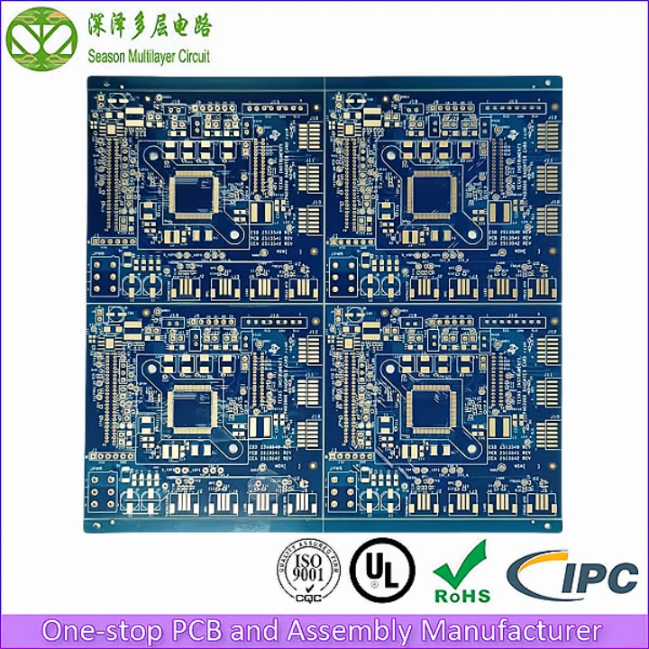
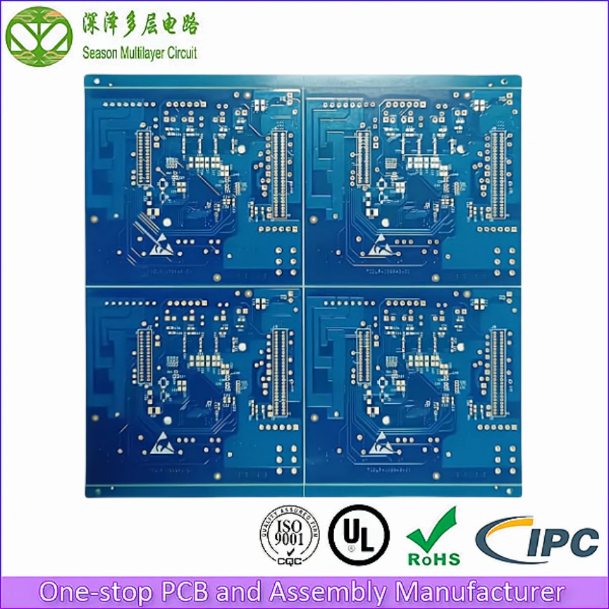
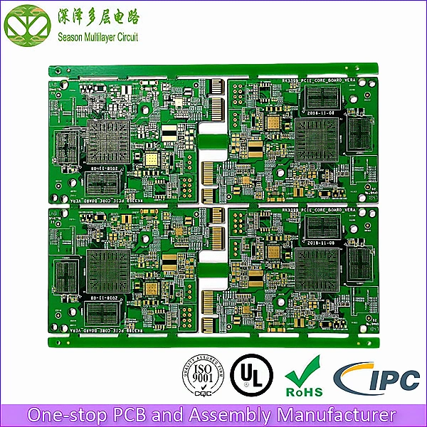
4 layer Automotive pcb

PCB prototyping
Layer Count: 4L
Material: FR4 Tg150
Board Thickness: 1.6mm
Panel Size: 162.56*159.86mm/4
Outer Layer Copper Thickness: 1OZ
Inner Layer Copper Thickness: 1OZ
Min Via Diameter: 0.20mm
Trace Width/Spacing: 4/4mil
Surface Finish: 2U’’ENIG
Automotive-grade PCB compliant with halogen-free requirements. Designed for automotive electronic components, offering stable performance, cost-effectiveness, fast lead time , and premium technical support.


Automotive PCBs: Engineering Excellence for Next-Generation Vehicles
Introduction
The automotive industry’s rapid evolution toward electrification, autonomy, and connectivity has thrust printed circuit boards (PCBs) into the spotlight. As vehicles transform into sophisticated electronic platforms, automotive PCBs have become the unsung heroes, enabling everything from battery management in electric vehicles (EVs) to real-time data processing in autonomous driving systems. This article delves into the technical intricacies, material advancements, and innovative manufacturing processes that define modern automotive PCBs, with a focus on industry leaders like Season Multilayer Circuit, renowned for their expertise in high-reliability solutions.
1. The Strategic Importance of Automotive PCBs
1.1 Powering the Electric Revolution
Electric vehicles rely on PCBs to manage high-voltage systems, including:
- Battery Management Systems (BMS): Monitoring cell voltages (±1mV accuracy) and thermal conditions.
- Motor Controllers: Switching currents up to 500A using silicon carbide (SiC) or gallium nitride (GaN) FETs.
- On-Board Chargers (OBC): Enabling fast charging (22kW+) with 95% efficiency.
PCBs for EVs demand 6 oz copper layers and arc-resistant substrates to handle extreme electrical and thermal loads.
1.2 Enabling Autonomous Driving
Autonomous vehicles require PCBs capable of processing terabytes of data daily:
- Sensor Fusion Modules: Integrating radar (77GHz), LiDAR (1550nm), and cameras with ≤4μm alignment accuracy.
- Centralized Domain Controllers: 20+ layer HDI boards supporting NVIDIA Orin or Qualcomm Snapdragon Ride platforms.
2. Material Innovations Driving Performance
2.1 High-Frequency Substrates
To support 5G-V2X and ADAS, materials like Rogers RO4835™ (ε<sub>r</sub>=3.3) and Panasonic Megtron 6 are replacing standard FR4, reducing signal loss by 30% at 77GHz.
2.2 Thermal Management Solutions
- Insulated Metal Substrates (IMS): Aluminum-core PCBs with 24W/mK thermal conductivity for EV inverters.
- Ceramic-Based PCBs: Used in 800V SiC systems to withstand temperatures exceeding 150°C.
2.3 Sustainability in Materials
Halogen-free laminates (e.g., Isola I-Tera® MT40) and lead-free finishes (e.g., ENIG 2U’’) align with EU RoHS and IATF 16949 standards.
3. Cutting-Edge Manufacturing Technologies
3.1 High-Density Interconnect (HDI)
HDI technology, a specialty of Season Multilayer Circuit, enables:
- Microvias: 0.10mm laser-drilled vias for 16-layer ADAS controllers.
- 4/4 mil Trace/Space: Critical for GPU and memory module routing.
3.2 Embedded Component Technology
Resistors and capacitors embedded within PCB layers reduce board size by 25% while improving signal integrity.
3.3 Additive Manufacturing
- 3D-Printed Flex PCBs: Conformal designs for curved displays and LED lighting.
- Aerosol Jet Printing: Precision deposition of conductive traces on non-planar surfaces.
4. Rigorous Quality Assurance for Automotive Reliability
4.1 Testing Protocols
- Thermal Shock Testing: 5,000 cycles (-55°C ↔ +125°C) per AEC-Q100.
- Vibration Testing: 20G shocks (ISO 16750-3) to simulate harsh driving conditions.
- CAF Resistance: 1,000 hours at 85°C/85% RH to prevent electrochemical failures.
4.2 Advanced Inspection
- 3D AOI: Detects defects as small as 10μm in HDI boards.
- X-Ray Inspection: Validates 100% via fill in BGA components.
5. Case Study: Season Multilayer Circuit’s Automotive Solutions
5.1 High-Speed ADAS Controllers
Season Multilayer Circuit delivered a 22-layer HDI PCB for a Tier-1 automotive supplier, featuring:
- 0.15mm microvias and 3/3 mil traces for NVIDIA DRIVE Orin.
- Low-loss materials (Df=0.002) for 112Gbps SerDes interfaces.
5.2 EV Power Electronics
6 oz copper, 10-layer PCB for an 800V SiC inverter achieved:
- 2W/in² heat dissipation using aluminum-clad substrates.
- AEC-Q100 Grade 1 certification for -40°C to +150°C operation.
5.3 Rapid Prototyping Capabilities
Leveraging 24/7 manufacturing lines, Season Multilayer Circuit reduces lead times to 5 days for automotive prototypes without compromising quality.
6. Future Trends Shaping Automotive PCBs
6.1 Heterogeneous Integration
Merging PCBs with System-in-Package (SiP) designs to integrate AI accelerators and photonic engines.
6.2 Photonic PCBs
Embedded silicon photonics for optical data transmission, reducing latency in autonomous systems.
6.3 AI-Driven Manufacturing
Machine learning algorithms optimizing DFM (Design for Manufacturing) and defect detection.
Conclusion
Automotive PCBs stand at the intersection of innovation and reliability, underpinning the industry’s shift toward smarter, cleaner, and safer mobility. Companies like Season Multilayer Circuit exemplify engineering excellence through their mastery of HDI technology, stringent quality controls, and agility in meeting OEM demands. As vehicles evolve into data centers on wheels, the role of automotive PCBs will only grow in complexity and importance, driving advancements that redefine transportation for decades to come.


