There have been many studies of the causes of tombstoning; some published, some not. They tend to focus on a single process parameter as the root cause of tombstoning. However, there is no single process change that is a sure cure for tombstoning! Those that claim otherwise are either uninformed or trying to sell you something. Rather than limiting your view to a single solution, Heros Electronics recommends you heed all of the studies. Like pieces of a puzzle, each study does not reveal the whole picture, but looked at all together, the picture is clear.
The issue of tombstoning has risen to prominence because, while components and assemblies have become much smaller over the last decade, overall assembly processes have remained much the same. As components become smaller, so should your process windows.
There was a time when a type II solder paste and chemically etched stencil were acceptable for almost all PCB assemblies. Throughout the 1990’s, type III paste and laser cut stencil became the norm. For those using micro-components today, a type IV paste and electro-formed stencil are quickly becoming a prerequisite. Likewise, equipment that can place components within plus or minus 2 or 3 thousandths (while suitable in its day) is no longer acceptable when placing 0201’s or even 01005’s. Ovens too are becoming more accurate as well.

Why does a component tombstone?
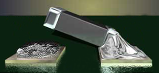
As the flux and solder alloy liquefy and wet to each side of a component, they apply small amounts of torque through surface tension. The torque applied by the surface tension of liquid flux and solder has traditionally been a fringe benefit as slightly misplaced components were pulled to center.
However, this friend has become a foe in modern electronics assembly for tombstoning is caused by minute differences in wetting force from one side of a component to the other. When there is a sufficient imbalance in torque, relative to the mass of the component, the component is tipped upright (tombstoned), consigning the product to either scrap or rework.

Chip components have gotten much smaller over the years with many weighing in the milligrams. The same torque that once helped alignment now has the power to tombstone components. The only way to completely eliminate the tombstoning effect is to tighten your process. There are many process variables that actively contribute to tombstoning. These include, but are not limited to, trace/board design, pad design, component and board oxidation, solder paste, stencil design, print process, placement process, and reflow process. Appropriate modification of one or more of these process variables will reduce or eliminate tombstoning.
Key tombstoning variables
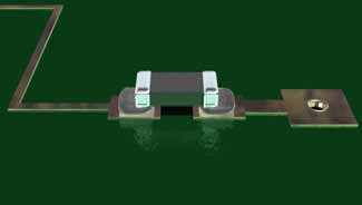
Trace/Board Design – When board designers are laying out a circuit board, manufacturability considerations are often unknown or ignored. Having established that wetting force imbalance causes tombstoning, one of the primary causes for imbalance is the difference in temperature and, correspondingly, the difference in time of reflow between the two pads the chip sits on.

Example: if Pad 1 is connected to a wide trace, ground plane, or other heat sinking element. Pad 2 is connected to a thinner trace or less massive circuitry element. Pad 2 will often be hotter than Pad 1 and reflow before Pad 1. This temperature difference result in a reflow timing difference. When Pad 2 wets first, the wetting force from Pad 2 may be enough to overcome the force from Pad 1 resulting in a tombstoned component.
Pad Design – Mechanical advantage also plays a role in both tombstoning and skewing for the same reasons. The larger the pad relative to the size of the component, the longer the “lever” that the liquid flux and solder can apply. When a pad is too wide, imbalance in force between side fillets will skew the component. When a pad is too long it lends mechanical advantage applied by the toe fillet making it easier to tombstone the component. Chip component pads should be no larger than necessary to meet mechanical and inspection requirements. In some cases, visual inspection requirements for fillet height will prevent the successful elimination of tombstoning due to restrictions on other aspects of the process.
Component and Board Oxidation – Oxidation on either pad or component surfaces will cause slight delays in wetting. The difference in wetting time from one pad to the other can cause tombstoning. Quality products and proper storage practices will help to eliminate this factor.
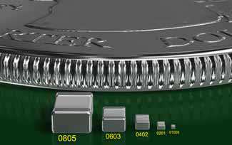
Component Geometry – Capacitors, inductors and other “thick” chip components are statistically more likely to tombstone than resistors and other “thin” chip components. The risk of tombstoning is larger for the same reason as for oversize pads. The distance that the flux and solder wet up the termination adds to mechanical advantage. Component size and mass also play a key role. The lighter the component, the less force it takes to tombstone. A process that is tombstone free with 0603 components may be unsuited to 0402 components. As newer, smaller chips are introduced into your production process, incremental changes may be required to deal with the new challenge.

From left to right: 0805, 0603, 0402, 0201, 01005
Solder Paste – Solder paste is actually two independent materials: flux and alloy. In rare circumstances, particularly bad flux formulations do not provide sufficient tack just prior to and during reflow. Side by side comparisons of pastes is required to identify differences in performance. With regards to alloy, it turns out that there is a difference in performance between eutectic alloys. Eutectic alloy changes state from solid to liquid all at once at a single temperature, developing full surface tension suddenly. Non-eutectic alloys changes state gradually over a temperature range develop surface tension over a broader temperature range and apply surface tension in some proportion. Non-eutectic alloys such as Sn62/Pb36/Ag2 and Sn96/Ag3.0/Cu0.5 have correspondingly lower incidence of tombstoning than Sn63/Pb37 and other eutectic alloys. The larger the melting range, the lower the probability of tombstoning.
|
Alloy: |
Solidus(°C) |
Liquidus(°C) |
|
Sn42 Bi58 |
-E- |
138 |
|
Sn43 Pb43 Bi14 |
144 |
163 |
|
Sn62 Pb36 Ag2.0 |
179 |
189 |
|
Sn63 Pb37 |
-E- |
183 |
|
Sn60 Pb40 |
183 |
191 |
|
Sn96.3 Ag3.0 Cu0.5 Sn96.3 Ag3.7 Sn100 Sn95 Sb5 |
217 -E- MP 232 |
219 221 232 240 |
|
Sn95 Ag5 |
221 |
245 |
|
Sn10 Pb88 Ag2.0 |
268 |
290 |
|
Sn5 Pb92.5 Ag2.5 |
287 |
296 |
|
Sn10 Pb90 |
275 |
302 |
|
Sn5 Pb95 |
308 |
312 |
|
-E-: Eutrctic MP: Melting point Green Color: Lead free |
||
Stencil Design – Stencil design has two elements: aperture design and stencil technology choice. Stencil aperture design determines two things: paste volume printed and paste location. A good stencil design will place only as much solder paste as is required. Too much paste will results in too tall a fillet and greater torque during liquefaction of the solder. A good design also places the solder in a location that ensures appropriate component to paste overlap. With too little overlap, there may be inadequate adhesion on the pad that reflows second. With too much overlap, solder beads/balls show up on the side of chip components. Stencil technology defines the expected paste release characteristics. In order of increasing paste release performance there is chemically etched stencils, laser cut stencils, and electroformed stencils.
Electropolishing and secondary plating of chemically etched and laser cut stencils has been proven to improve their paste release performance. Print Process – One factor that has been shown to dramatically decrease tombstoning is the quality of print. With more uniform deposits, adhesion is more even from pad to pad. For 0201 apertures and others similar in size, Type IV solder paste has been proven to significantly improve print quality. Print settings should be optimized for maximum print definition and uniformity.
Placement Process – If the component is placed more to one side or another, it will allow more surface tension to be applied to that side, and the component can stand up. If the component is not placed with sufficient pressure, it will begin to tip as wetting occurs, and if it is pushed too deeply into the paste, the paste will be displaced, and (again) uneven wetting may occur.
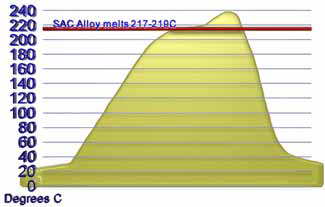
Reflow Process – The reflow process is probably the most significant contributor to tombstoning. When a board design with tombstone friendly features is sent through the oven, how the board is heated can make a tombstone problem either better or worse. To minimize tombstoning, the goal is to ramp temperature such that the solder alloy liquidus is achieved uniformly for all pairs of pads the board. This means that the whole board should be brought to a temperature just below liquidus, and then slowly ramped up to reflow. By keeping wetting forces equal on both sides of a chip component, it is less likely to tombstone. For most products, a ramp rate of around 1°C per second is adequate insurance against reflow induced tombstoning. More difficult products may require slower ramp rates with some as low as 0.33°C per second.
