One-stop PCB and Assembly Manufacturing Service
Season Multilayer Circuit, a subsidiary of the 998PCB Group, stands as a leader in PCB manufacturing. We specialize in advanced HDI, multilayer PCBs, FPCs, and rigid-flex boards, complemented by SMT processing and full-spectrum PCBA OEM/ODM services. Understanding your dual pursuit of efficiency and quality, we prioritize rapid PCB prototyping and timely delivery to accelerate your project’s time-to-market.
Our one-stop PCB and PCBA manufacturing solutions deliver unparalleled convenience and efficiency. With competitive pricing and swift lead times, we ensure premium-quality products that exceed value expectations. Season Multilayer Circuit remains your trusted partner, committed to empowering your success through cost-effective solutions and exceptional service.
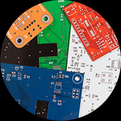
PCB Manufacturing
√ 2-30layer Fast PCB sample
√ HDI PCB(Any layer interconnection)
√ High frequency PCB (low Dk/Df)
√ High speed PCB & Rigid flex
√ 1000-1500mm long PCB board
√ Extra thick PCB(20mm)
√ 100% Quality guarantee
√ HDI PCB(Any layer interconnection)
√ High frequency PCB (low Dk/Df)
√ High speed PCB & Rigid flex
√ 1000-1500mm long PCB board
√ Extra thick PCB(20mm)
√ 100% Quality guarantee
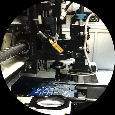
PCB Assembly
√ Surface mounted technology (SMT)
√ Pin-through holes (PTH)
√ Reflow & wave soldering
√ Hand soldering
√ IC burning & programming
√ RoHS compliant (lead-free)
√ Dust-free workshop
√ Pin-through holes (PTH)
√ Reflow & wave soldering
√ Hand soldering
√ IC burning & programming
√ RoHS compliant (lead-free)
√ Dust-free workshop
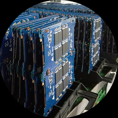
Turnkey PCB and Assembly
√ One-stop PCB and assembly
√ Original components sourcing
√ Solder paste stencil production
√ 1-24h quick quote for BOM prices
√ 2 shifts a day & fast shipping
√ 100% PCBA test without defect
√ No risk
√ Original components sourcing
√ Solder paste stencil production
√ 1-24h quick quote for BOM prices
√ 2 shifts a day & fast shipping
√ 100% PCBA test without defect
√ No risk
Today’s Special Offer For PCB Samples
Season Multilayer Circuit provides discounted PCB samples to new customers every day, and all discounted samples are valid for the same day. Welcome to purchase.
8L PCB Sample
√Within 0.3 ㎡ ( within 100 pcs)
√No special processes
√Surface ENIG/OSP/HASL
√Default board Fr4 Tg150
√Excluding shipping costs
√Thickness 0.8-1.6mm
√No special processes
√Surface ENIG/OSP/HASL
√Default board Fr4 Tg150
√Excluding shipping costs
√Thickness 0.8-1.6mm
$280.00
10L PCB Sample
√Within 0.3 ㎡ ( within 100 pcs)
√No special processes
√Surface ENIG/OSP/HASL
√Default board Fr4 Tg170
√Excluding shipping costs
√Thickness 0.8-1.6mm
√No special processes
√Surface ENIG/OSP/HASL
√Default board Fr4 Tg170
√Excluding shipping costs
√Thickness 0.8-1.6mm
$350.00
12L PCB Sample
√Within 0.3 ㎡ ( within 100 pcs)
√No special processes
√Surface ENIG/OSP/HASL
√Default board Fr4 Tg170
√Excluding shipping costs
√Thickness 0.8-1.6mm
√No special processes
√Surface ENIG/OSP/HASL
√Default board Fr4 Tg170
√Excluding shipping costs
√Thickness 0.8-1.6mm
$420.00
HDI PCB(1+4+1)
√Within 0.3 ㎡ ( within 100 pcs)
√No special processes
√Surface ENIG/OSP/HASL
√Default board Fr4 Tg150
√Excluding shipping costs
√Thickness 0.8-1.6mm
√No special processes
√Surface ENIG/OSP/HASL
√Default board Fr4 Tg150
√Excluding shipping costs
√Thickness 0.8-1.6mm
$350.00
HDI PCB(1+6+1)
√Within 0.3 ㎡ ( within 100 pcs)
√No special processes
√Surface ENIG/OSP/HASL
√Default board Fr4 Tg150
√Excluding shipping costs
√Thickness 0.8-1.6mm
√No special processes
√Surface ENIG/OSP/HASL
√Default board Fr4 Tg150
√Excluding shipping costs
√Thickness 0.8-1.6mm
$420.00
HDI PCB(2+2+2)
√Within 0.3 ㎡ ( within 100 pcs)
√No special processes
√Surface ENIG/OSP/HASL
√Default board Fr4 Tg170
√Excluding shipping costs
√Thickness 0.8-1.6mm
√No special processes
√Surface ENIG/OSP/HASL
√Default board Fr4 Tg170
√Excluding shipping costs
√Thickness 0.8-1.6mm
$490.00
How To Order a Special Sample
1.Capture a Screenshot and Email Us: Please take a screenshot of the special-priced PCB sample and send it to us via email. Simultaneously, provide us with the Gerber files and manufacturing requirements.
2.Review of Special Pricing Conditions: We will assess your files and requirements to determine if they meet the criteria for the special pricing.
3.Quotation and Invoice: Upon verification of compliance, we will provide you with a quotation for the special-priced PCB sample along with a commercial invoice.
4.Payment Confirmation and Production Arrangement: Await your confirmation of payment, and upon receipt, we will proceed to arrange for production.
Our Top 10 Advantages
We have a professional manufacturing team with rich experience and expertise, and have been engaged in the pcb industry for nearly 20 years. We have served more than 8,000 customers and achieved a customer satisfaction rate of more than 98%. We provide customers with a variety of pcb products to meet various needs.
1.Reliable PCB manufacturing and assembly
Season Multilayer Circuit has a good reputation in the industry for its reliable manufacturing and assembly capabilities. We have first-class equipment, advanced production technology and efficient operation processes to ensure that the PCB manufacturing and assembly process is both reliable and efficient. In addition, we also provide comprehensive quality assurance and after-sales service to meet the various needs of our customers.
2.High quality PCB manufacturing
Season Multilayer Circuit is very persistent in its pursuit of quality. We use high-quality raw materials and strict quality control standards to ensure that every PCB meets the highest quality requirements. In the manufacturing process, we pay attention not only to the performance and reliability of our products, but also to the details and aesthetics, thus providing our customers with high-quality and durable PCB components.
3.On-time PCB delivery time
Season Multilayer Circuit takes customers’ project timelines very seriously and is committed to delivering PCB orders on time. We have an efficient logistics system and complete storage facilities to ensure that orders can be processed and shipped in a timely manner. In addition, we offer flexible delivery schedules to meet the specific needs of our customers.
4.Well-funded PCB enterprises
Season Multilayer Circuit is a well-funded business, which allows us to carry out mass production and offer competitive prices to our customers. In addition, our financial strength is also used for continuous technology research and development and equipment upgrades to maintain industry leadership. This financial position also gives us the ability to provide flexible financial solutions to meet the various needs of our customers.
5.24 hours technical support
Season Multilayer Circuit provide 24-hour online technical support to ensure that customers can get timely answers when they encounter problems. Our technical support team consists of experienced engineers who are able to provide customers with accurate and efficient solutions. Whether in the design phase or in the production process, the technical support team always maintains close contact with the customer to solve various problems and doubts in a timely manner.
6.PCB Instant quote
Season Multilayer Circuit provide customers with instant, accurate quotes. As long as the customer provides the necessary Gerber documents and system requirements, we will provide the quotation within 0.5-2 hours, which greatly saves the customer’s time and effort. At the same time, in order to meet the needs of different customers, I can also provide expedited price assessment, which can provide customers with accurate quotes within 0.5 hours.
7.PCB order status tracking
Through the customer service staff of Season Multilayer Circuit, customers can check the status of orders, delivery status and logistics information at any time. This allows the customer to accurately grasp the dynamics of the order and thus better plan production and schedule. At the same time, customers can also check the order details at any time through the order tracking system, including order number, order time, product name, quantity, etc.
8.No minimum PCB order requirement
Season Multilayer Circuit does not set a minimum order quantity limit, and customers are free to place orders according to actual needs. This provides great convenience for small or experimental projects, reducing costs and risks for the client. No matter the size of the order, Season Multilayer Circuit is willing to cooperate with customers and provide quality service.tes within 0.5 hours.
9.Project fees are waived in bulk
Season Multilayer Circuit promises free engineering costs for bulk orders, which saves customers additional engineering costs, and at the same time, test fixture costs can be waived for bulk orders up to a certain number. In addition, we provide free technical support and consulting services to help customers solve engineering problems and provide solutions.
10.PCB files are free to check
In order to ensure that customers’ PCB design documents are correct, Season Multilayer Circuit offers a free document inspection service. Their technical team will carefully examine the customer’s documentation and point out possible problems, ensuring a smooth PCB manufacturing process. This service helps to identify potential problems in advance and avoid errors or delays in the production process.
0
Cumulative customer service
0
Customer satisfaction
0
Engaged in PCB industry
About Season Multilayer Circuit
Season Multilayer Circuit, established in 2006 and affiliated with the 998PCB Group, has been providing high-end HDI, expedited HDI samples, expedited PCB samples, high-speed PCB, high-frequency PCB, FPC, rigid-flex PCBs, and one-stop PCBA manufacturing services to the global market for nineteen years. Our products are popular domestically and are exported to global markets including Europe, America, Japan, South Korea, and the Asia-Pacific region.
We have always adhered to the principles of pursuing excellence, customer satisfaction, full participation, and continuous improvement. With a customer-centric approach, we provide stable product quality, timely delivery, and win customer satisfaction through excellent service, aiming for sustainable operation. Over the past nineteen years, we have served more than 8,000 customers, with a customer satisfaction rate of over 98%. We have earned long-term trust and praise from our customers through fast delivery, stable quality, and reasonable prices.
We have successively obtained certifications such as ISO9001-2000, UL, ISO9001-2008, ISO14001-2004, CQC, and TS/16949. Our products are widely used in high-tech industries including communication equipment, computers, smart homes, automotive electronics, industrial control, power electronics, medical equipment, security electronics, aerospace, and more.
Latest Release
As a global manufacturer of PCBs, Season Multilayer Circuit will periodically share technical knowledge on PCB and PCBA products. We hope this information will be of assistance to you. If you encounter any other issues during production, please feel free to contact us, and we will provide you with further assistance.

Industrial PCBA
See More PCBAs

Navigation Core Board PCBA
See More PCBAs
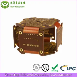
6 Layer Rigid-flex PCB
See More Rigid-flex-pcbs
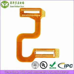
Double Sided Medical FPC Proofing
See More Rigid-flex-pcbs


