Production Process of HDI PCB
The production process of HDI (High-Density Interconnect) circuit boards is a highly sophisticated and precise procedure involving design, manufacturing, inspection, testing, and delivery. Rigorous quality control ensures that the final product meets performance and functional requirements before reaching customers. Below is a detailed breakdown using an 8-layer, 2-step HDI (2+4+2) board as an example. This article is lengthy, so you may want to bookmark it for later reference.
1. Cutting (Panelization)
The raw copper-clad laminate is cut into processable sizes based on engineering specifications. CAM engineers panelize the Gerber files (provided as single Units) into Sets and combine multiple Sets into a Panel to optimize production efficiency.
- Unit: Customer-designed single-board pattern (Gerber file).
- Set: Multiple Units arranged with tooling borders for batch processing.
- Panel: Large boards (e.g., 915×1,220mm / 36”×48”) formed by combining Sets to maximize material utilization.
2. Inner Layer Fabrication
The inner layer circuit pattern is transferred onto the copper-clad laminate through photolithography:
- Lamination: Apply photosensitive dry film to the copper surface.
- Exposure & Development: UV light cures exposed areas, forming a protective mask.
- Etching & Stripping: Remove unprotected copper, leaving the circuit pattern.
Design Considerations:
- Minimum line width/spacing to avoid shorts or opens.
- Uniform copper distribution to prevent resin flow imbalance during lamination.
3. Inner Layer AOI (Automated Optical Inspection)
Optical scanning detects defects (e.g., opens, shorts) for early repair, preventing defective products from advancing to subsequent stages.
4. Browning/Black Oxidation Treatment
The copper surface undergoes oxidation to:
- Remove contaminants (oil, impurities).
- Increase surface roughness for better resin adhesion.
- Convert non-polar copper to polar CuO (black) or Cu₂O (brown), enhancing bonding strength.
5. Lamination

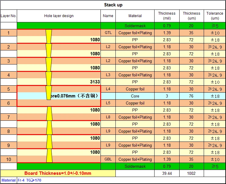
Multiple layers (copper foil, prepreg, inner cores) are bonded under high temperature and pressure to form a unified structure:
- Stackup Symmetry: Asymmetric designs cause uneven stress distribution, leading to warpage.
- Resin Flow Control: Uneven copper density affects resin distribution, requiring balanced layouts during design.
6. Buried Via Drilling

Mechanical drilling (≥6mil hole diameter) creates buried vias (e.g., layers 3–6 in an 8-layer board). Design constraints:
- Avoid intersecting blind/buried vias (e.g., 3–5 and 4–6 layers) to reduce complexity and cost.
- Symmetric via placement minimizes production challenges.
7. Plating Through Holes (PTH)
Holes are metallized to ensure conductivity:
- Desmearing: Remove resin residues from hole walls.
- Electroless Copper Deposition: Chemically coats the hole walls.
- Electroplating: Thickens the copper layer for reliability.
Aspect Ratio: Critical for plating quality (board thickness ÷ hole diameter). Higher ratios increase defect risks (e.g., micro-opens).
8. Resin Plugging & Second Inner Layer Fabrication

Buried vias are filled with resin, planarized, and polished. The board then returns to inner layer processing to create circuits for layers L3 and L6.
9. Second Lamination
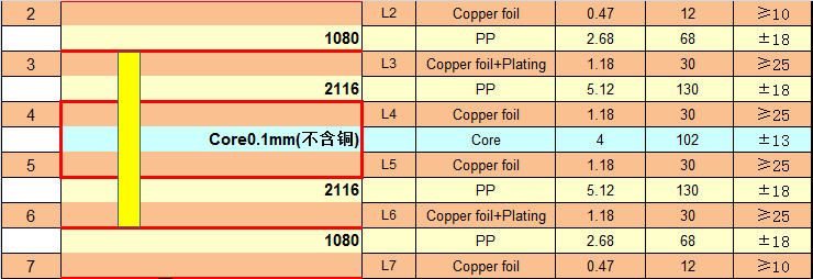
The board is pressed again to form a 6-layer structure (L2 and L7 layers added). Key Challenges:
- Thin HDI insulation layers (e.g., RCC materials) complicate lamination.
- Blind via alignment must avoid overlapping with outer layer traces to prevent open circuits.
10. Laser Drilling
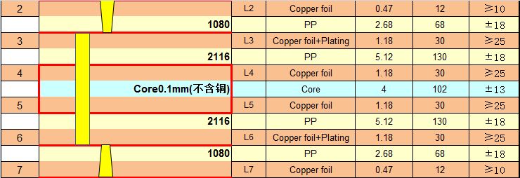
Laser drilling creates microvias (3–6mil diameter) for HDI interconnects:
- Aspect Ratio: ≤1:1 (e.g., 0.1mm hole depth for 0.1mm diameter).
- Speed: 100–200 holes/second, depending on hole size.
Post-Drilling Treatment: High-pressure water cleaning removes scorch residue from laser-drilled holes.
11. Blind Via Filling & Electroplating
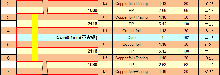
Blind vias are plated and filled to ensure conductivity:
- Stacked Vias: Require specialized plating/filling techniques (high cost).
- Staggered Vias: 80% filling suffices for functional requirements.
12. Sub-Outer Layer Fabrication
The L2 and L7 layers undergo inner layer processes (dry film, exposure, etching). Multiple alignment steps introduce cumulative errors, increasing scrap rates for 2-stage HDI boards.
13. Third Lamination
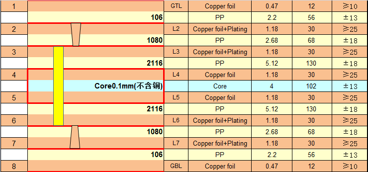
Final lamination adds the outermost layers (L1 and L8). The board now transitions to standard 8-layer through-hole processes.
14. Second Laser Drilling
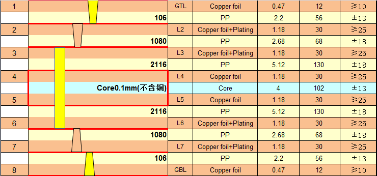
Additional laser drilling creates interconnects for outer layers.
15. Through-Hole Drilling
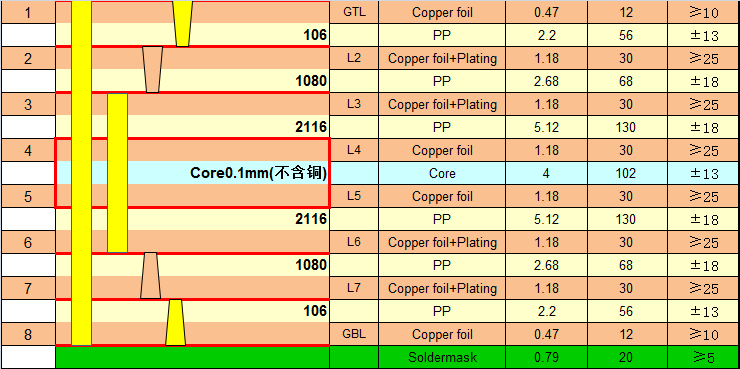
Mechanical drilling creates through-holes for final interlayer connections.
16. Final Plating (PTH)
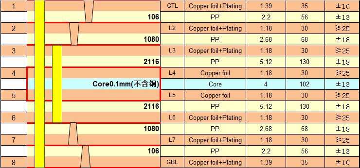
All holes (blind and through) are metallized, completing HDI-specific processes.
17. Outer Layer Pattern Imaging
Outer layer circuits are transferred using:
- Negative Film: Cured areas become circuits after etching.
- Positive Film: Non-cured areas are plated with copper/tin before etching.
18. Outer Layer AOI (Automated Optical Inspection)
19. Solder Mask
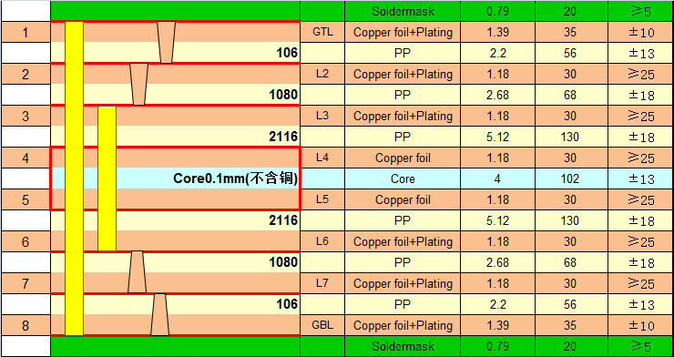
- Concept: The solder mask process involves adding a protective layer (solder mask ink, commonly called “green oil”) to the PCB surface. Its functions include preventing unintended soldering on conductor traces, avoiding short circuits caused by humidity/chemicals, protecting against open circuits/insulation failures during production/assembly, and resisting harsh environments to ensure PCB functionality.
- Principle: PCB manufacturers typically use liquid photoimageable solder mask (LPSM). The process resembles circuit pattern transfer, utilizing film masking and exposure to transfer solder mask patterns onto the PCB. Key steps:
Pre-treatment → Coating → Pre-baking → Exposure → Development → UV Curing → Thermal Curing
Critical parameters include solder mask alignment accuracy, green oil bridge width, via treatment methods, and solder mask thickness. Solder mask quality significantly impacts surface finish, SMT assembly, storage, and PCB lifespan. As a complex and time-consuming process, it is vital in PCB manufacturing.
Via design/treatment and solder mask appearance defects are key concerns for designers and QC engineers, respectively.
20. Silkscreen (Legend)
21. Surface Finish
Common surface finishes: ENIG (Electroless Nickel Immersion Gold), HASL (Hot Air Solder Leveling), OSP (Organic Solderability Preservative), ENIG+OSP (selective gold plating). Others include immersion silver, immersion tin, electroplated hard gold, and ENEPIG (Electroless Nickel Electroless Palladium Immersion Gold).
- ENIG: Applied after solder mask to exposed copper areas. Suitable for fine-pitch designs due to excellent flatness and coplanarity.
- Nickel thickness: ~5μm; Gold thickness: 0.025–0.076μm.
- Advantages: Stable gold layer, long shelf life (comparable to lead-tin).
- Disadvantages: Brittle joints if Au is too thick, “black pad” defects, and poor solderability if too thin.
- HASL: Dipping PCB in molten solder (lead-tin alloy or lead-free pure tin) followed by hot air leveling.
- Lead-based HASL: ~240°C; Lead-free HASL: ~300°C.
- Advantages: Excellent solderability and reliability.
- Disadvantages: Poor planarity, via plugging risks, high thermal stress causing warpage, and strict requirements for solder mask/laminate adhesion.
- OSP: Forms a thin organic anti-oxidation layer on bare copper.
- Advantages: Good solderability, flat surface, low cost.
- Disadvantages: Film easily scratched; degrades after multiple reflow cycles (unterminated pads may discolor/crack).
- Typically applied post-electrical testing to avoid film damage.
22. Routing (PCB Depanelization)
CNC machining separates individual PCBs (units/sets) from the production panel. Processes include:
- Outline milling, slot cutting, and V-scoring (if required).
- Key parameters: Outline tolerance, chamfer/radius dimensions, and edge clearance design rules.
23. Electrical Testing (E-test)
Tests for open/short circuits using:
- Bed-of-Nails Testing: Dedicated fixtures for specific PCBs (low cost) or universal fixtures (higher cost).
- Flying Probe Testing: Mobile probes test panelized PCBs pre-depanelization for efficiency.
24. Final Audit
25. Packaging
26. Shipment
The Production Process of HDI is an intricate and demanding operation, requiring exceptional precision across all stages. To ensure successful production, each process step must maintain a yield rate exceeding 99%, demanding rigorous quality standards and meticulous execution. Only through such uncompromising control can the final HDI boards meet the stringent performance and reliability requirements of advanced electronic applications.


